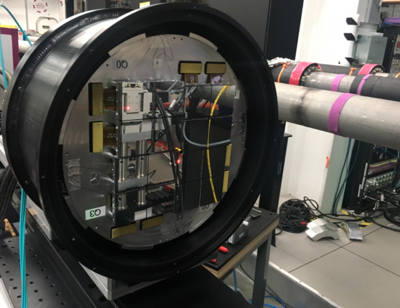
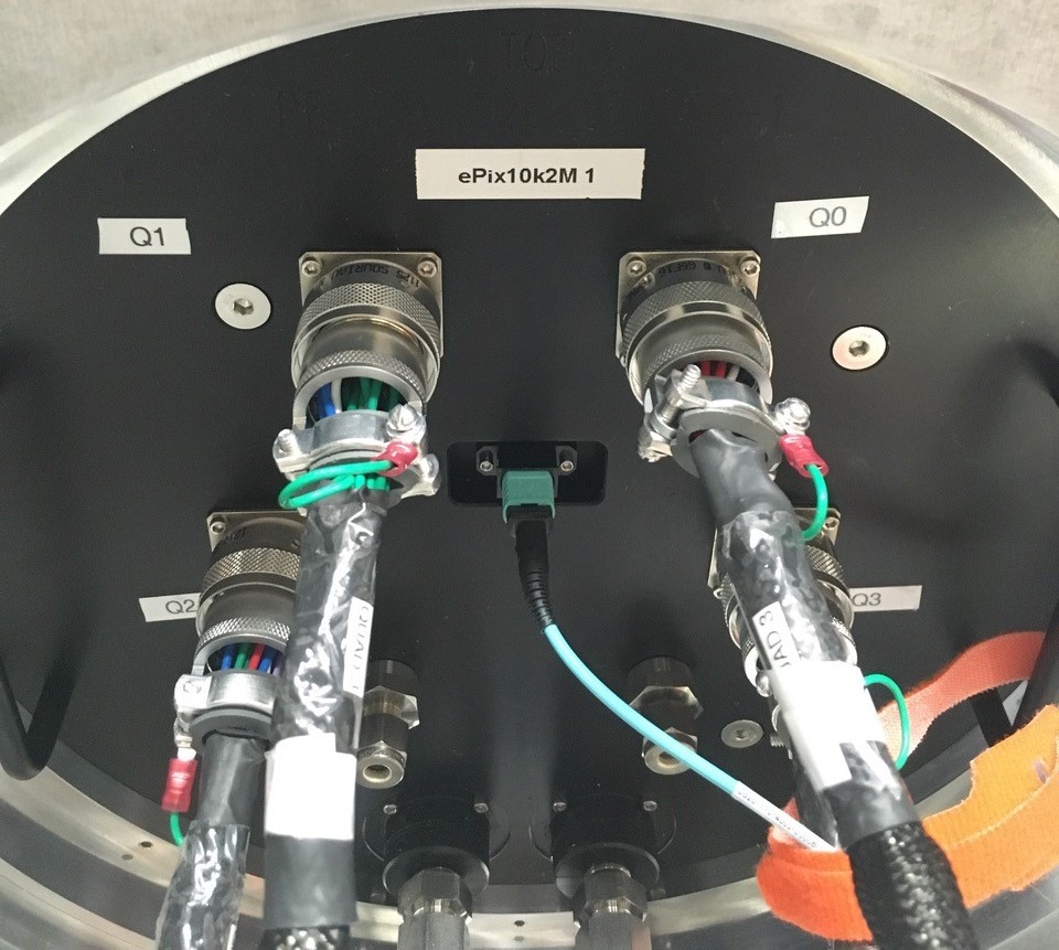
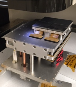
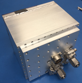
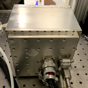
Two new detectors EPIX10KA2M and EPIX10KAQUAD are composed from EPIX10KA modules.
Content
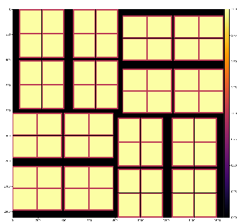
Geometry
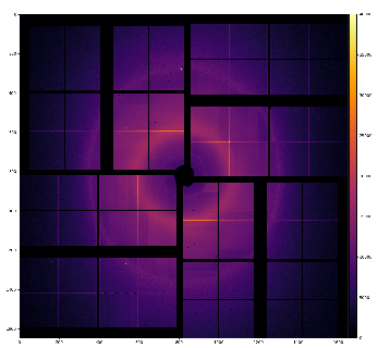
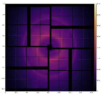
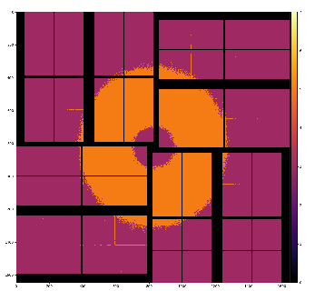
Plots and comments from Chris Kenny
Comments on epix10ka2m geometry from Chris Kenney
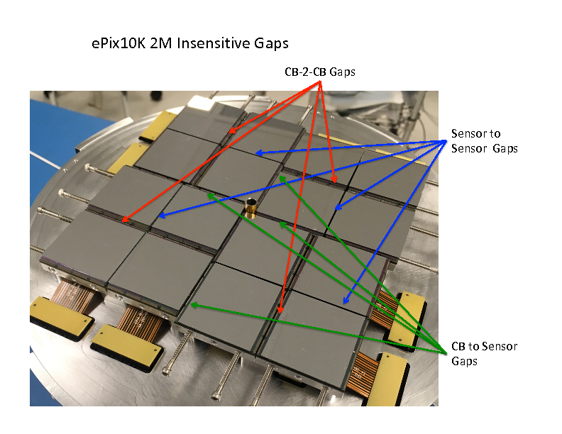
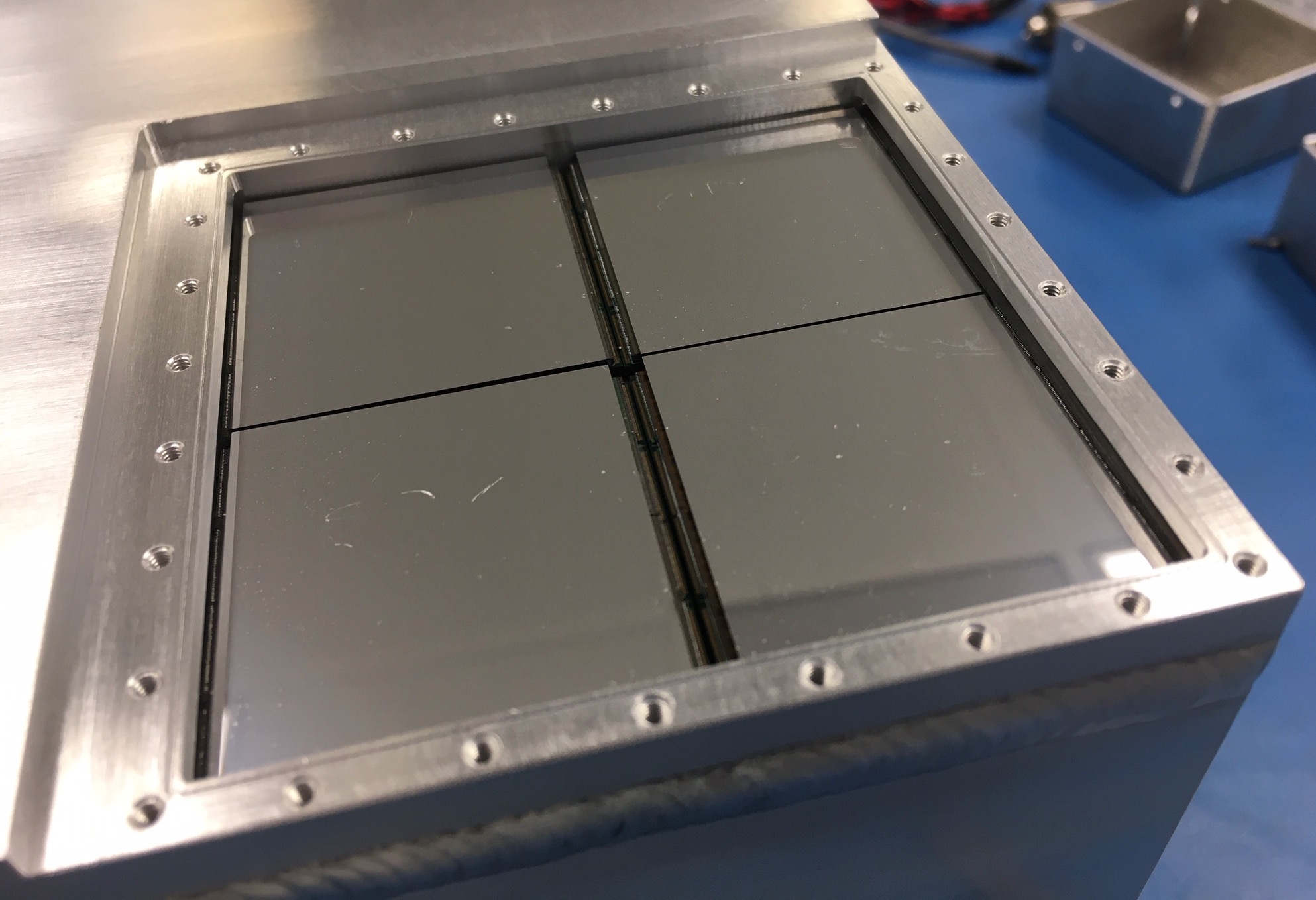
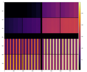
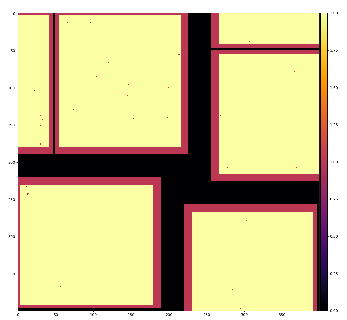
Kenney, Christopher J. 2018-11-12, 2:26 PM

Guide tube is 7mm outer diameter
We added polyimide tape that was 150 microns thick before application
to the tube.

But a decent estimate would be the mechanical edge-to-edge orthogonal
separation between sensor edges 7.3 mm.
We need to add about 1 mm for the guard rings on each sensor

So the orthogonal gap between active pixels on opposing quads across
the beam guide tube should be 8.3 mm

====
Kenney, Christopher J. 2018-11-12, 4:41 PM Blaj, Gabriel;Dubrovin, Mikhail;Kwiatkowski, Maciej

Very rough estimate of the gaps
There are 3 types of gaps
All are active pixel to active pixel
sensor to sensor ~ 1.6 mm
CB to CB ~ 6.4 mm
sensor to CB ~ 3.9 mm

====
CB = Carrier Board edges
Full camera image below
====
so 384 columns parallel to the balcony (the widest dead gaps)
and 352 orthogonal to the balcony (vertical direction)
epix10ka2m assembly
epix10ka2m-insensitive-gaps.pdf
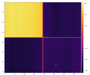
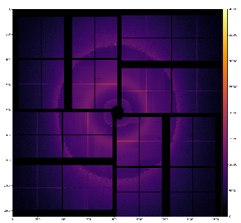
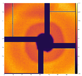
epix10ka sensor central region between 4 ASICs
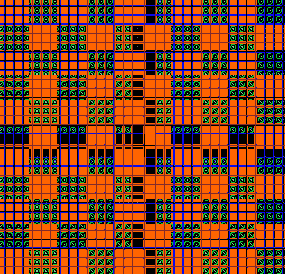
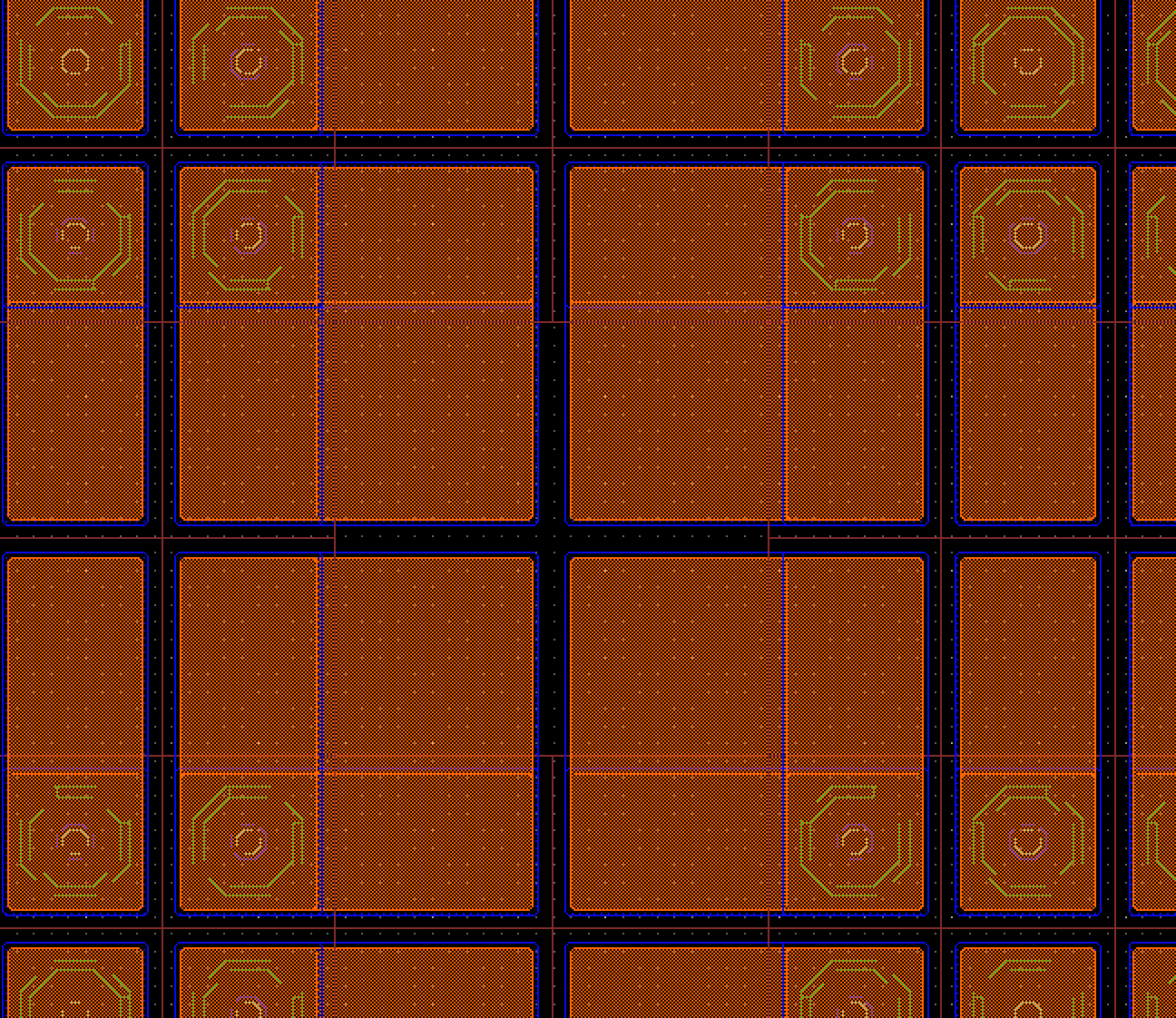
The internal gap between four ASICs in sensor,
pixel size 100 x 225 microns in area in both directions.
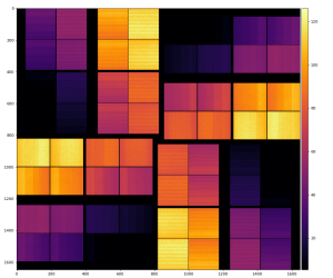
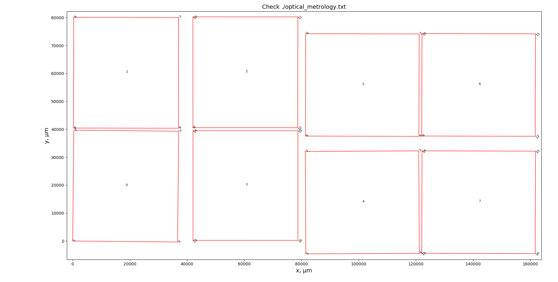
Metrology map from Chris Kenney
- 2018-11-18-epix10ka2m-metrology-map.pdf
- 2018-11-18-epix10ka2m-metrology-map.pptx
- 2018-11-15-Metrology-epix10ka2m.xlsx
Front and back side of the new detector epix10ka2m.1 from mfxc00118 2020-07-dd
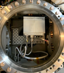
2020-10-04 MEC epix10kaquad 0 at optical metrology
2020-10-06 MEC epix10kaquad 0 front and back
2021-04-10 UED epix10kaquad
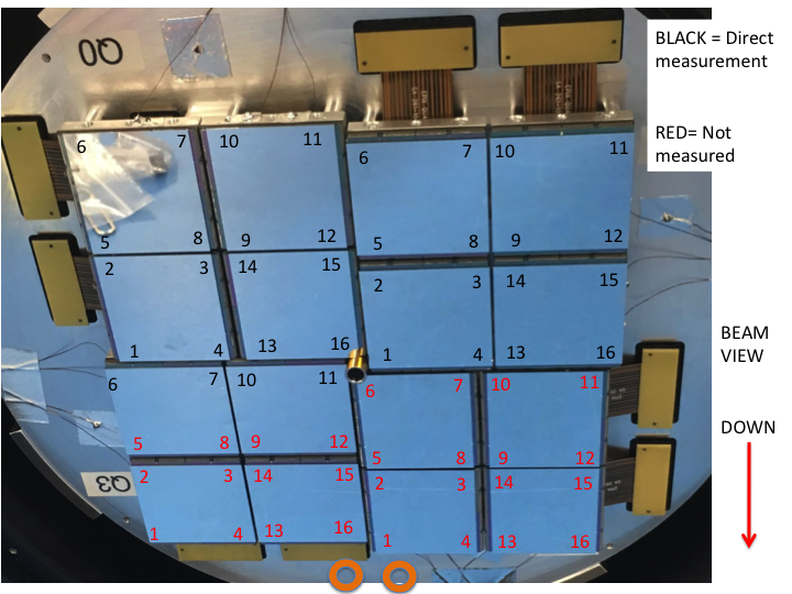
Comments on orientation of epix10ka2m parts from Matt
2018-11-19 orientation schema
Weaver, Matt
2018-11-19, 7:37 PMO'Grady, Paul Christopher;Dubrovin, Mikhail

Hi Mikhail,
We took radioactive source test
 runs today to verify the geometry.  We found that we were rotated by 90
 degrees, which matches the labeling on the back of the detector as well
 as the metrology picture from Chris Kenney.
The runs are
/reg/d/psdm/det/detdaq17/e968-r0131   - source unmasked (up to ~ event 10000), then masked vertically after ~ event 15000
/reg/d/psdm/det/detdaq17/e968-r0132   - source masked horizontally at bottom after ~ event 15000.

So, the picture is...
  //  (Epix10ka2m)
  //         |
  //  Quad 0 | Quad 1      Quad 2 is rotated  90d clockwise
  //  -------+--------     Quad 3 is rotated 180d clockwise
  //  Quad 3 | Quad 2      Quad 0 is rotated 270d clockwise
  //         |
  //
  //  (Quad 1)
  //         |
  //  Elem 0 | Elem 1
  //  -------+--------     No rotations
  //  Elem 2 | Elem 3
  //         |
  //
  //  (Elem 0)
  //         |
  //  ASIC 0 | ASIC 3
  //  -------+--------     No rotations
  //  ASIC 1 | ASIC 2
  //         |
  //
  //  (Elem 0-3 pixel array)
  //                    row increasing
  //                          ^
  //                          |
  //                          |
  //  column increasing <-- (0,0)
Preliminary geometry
in /reg/g/psdm/detector/data_test/calib/
/reg/g/psdm/detector/data_test/calib/Epix10ka2M::CalibV1/NoDetector.0:Epix10ka2M.0/geometry/0-end.data @      (epix10ka2m - entire detector)
/reg/g/psdm/detector/data_test/calib/Epix10kaQuad::CalibV1/NoDetector.0:Epix10kaQuad.0/geometry/0-end.data @  (epix10kaquad - one quad)
/reg/g/psdm/detector/data_test/calib/Epix10ka::CalibV1/MecTargetChamber.0:Epix10ka.1/geometry/0-end.data @    (epix10ka - one panel)
copy of geometry files in alignment examples /reg/g/psdm/detector/alignment/
/reg/g/psdm/detector/alignment/epix10ka2m/calib/Epix10ka2M::CalibV1/NoDetector.0:Epix10ka2M.0/geometry/0-end.data
/reg/g/psdm/detector/alignment/epix10kaquad/calib/Epix10kaQuad::CalibV1/NoDetector.0:Epix10kaQuad.0/geometry/0-end.data
/reg/g/psdm/detector/alignment/epix10ka/calib/Epix10ka::CalibV1/MecTargetChamber.0:Epix10ka.1/geometry/0-end.data
Optical metrology processing
Scripts for processing
CalibManager/app/
  optical_metrology_check
  optical_metrology_epix10ka2m
Results in
/reg/g/psdm/detector/alignment/epix10ka2m/calib-mfx-epix10ka2m-01-2018-11-15/
  2018-11-15-Metrology-epix10ka2m.xlsx
  2018-11-15-Metrology-epix10ka2m.txt
  2018-11-15-Metrology-epix10ka2m-corr.txt
  2018-11-15-geometry-epix10ka2m.txt - geometry file accounting for optical metrology data
  README-2018-11-15
Gain
Gain factors from charge injection default and measured
| gain | charge injection | current default | measured (ADU / keV) | 2020-08-03 Gabriel (ADU / keV) - use as default |
|---|---|---|---|---|
| L | 0.46 | 0.01 | 0.139 | 0.164 |
| M | 15. | 0.3(3) | 4.5 | 5.466 |
| H | 46.7 | 1 | 13.9 | 16.40 |
Gain factors default vs charge injection
- Detector/examples/ex_epix10ka_images.py
- XcsEndstation.0:Epix10ka2M.0
- charge injection gain factors were generated from exp=xcsx35617:run=544
- data with water ring for comparison exp=xcsx35617:run=528
- account relative factor 46.7
- selected rect [6, 120:170, 200:250]
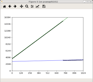
gain default: H / M / L = 1 / 0.33333 / 0.01
gain from charge injection:
| constants | Mean | RMS | RMS / MEAN |
|---|---|---|---|
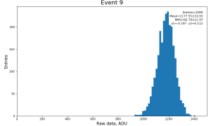
| default | 1117.7 | 62.72 | 0.05618 |
| charge injection | 1177.5 | 66.79 | 0.05672 |
Conclusion: in this test charge injection gainci constants do not improve gain factors comparing to default
Default gain correction factors
Test of the gain switching modes
offset calibration: exp=xcsx35617:run=544; its timestamp 20181129124822 faked for earlier dark calibrations by reference from 20180101000000
dark runs: 413, 416, 417, 420 of xcsx35617
gain factors M, H=1, L= 0.2, 0.25, 0.3, 0.33333, 0.4
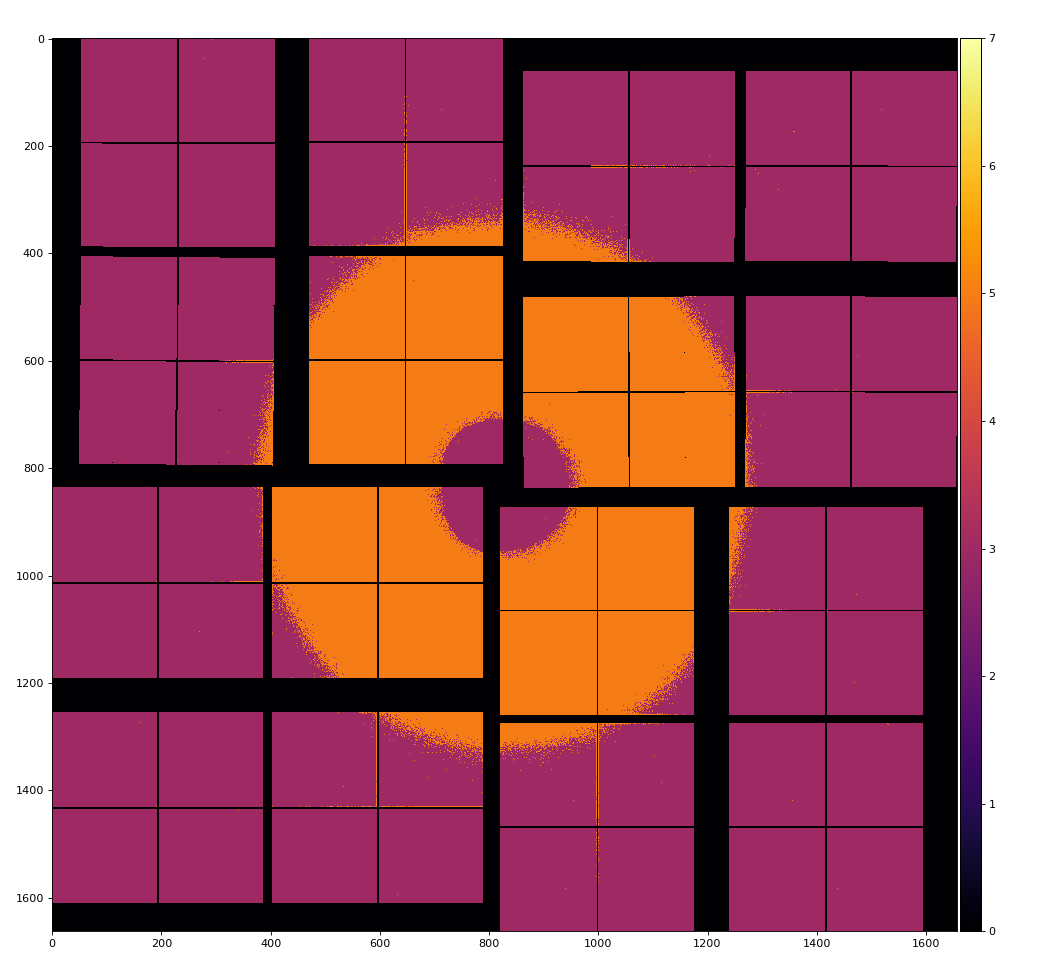
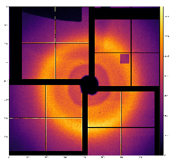
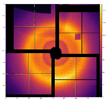
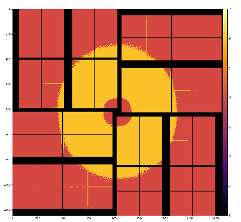
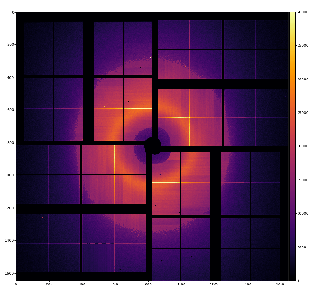
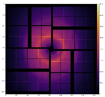
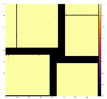
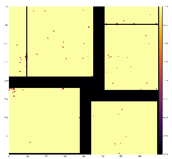
gain map images show that lateral and central-most pixels in mode H, M, "water ring" region pixels switched to L
data:
- AML: exp=xcsx35617:run=419, event 3
- AHL: exp=xcsx35617:run=414, event 3
Masks
mask_geo
mask_geo = det.mask_geo(par, mbits=3, width=10, wcentral=5)
- mbits = 1 - masks edges, +2 - masks central rows and columns.
- width - number of edge rows or columns to mask, def=1
- wcentral - number of central rows or columns to mask, def=1
plot for mask_geo + 1:
status_as_mask
- use pixel_status for exp=xcsx35617:run=544
- mask_status = det.status_as_mask(par, mode=0, indexes=(0,1,2,3,4))
- mode 0/1/2 masks zero/four/eight neighbors around each bad pixel
- indexes=(0,1,2,3,4) # indexes stand for FH, FM, FL, AHL-H, AML-M, respectively. Derived modes have the same status arrays.
found number of bad pixels
- 2802 for F gain modes and
- 3253 for all F + A mode
plots for mask_status + 1 for mode=0, 1 and 2:

Combined mask
mask = det.mask(par, calib=False, status=True, edges=True, central=True, width=10, wcentral=5, mode=0)
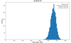
Calibrated data and mask
Image and spectrum for
- nda = calib_epix10ka_any(det, evt)
- nda *= det.mask(par, calib=False, status=True, edges=True, central=True, width=1, wcentral=1, mode=0)

Manual alignment on 2019-05-06
Data
Ring-data (npy) arrays were provided for xcsx35617 run 400 by Silke, available under
- /reg/g/psdm/detector/alignment/epix10ka2m/calib-mfx-epix10ka2m-01-2018-11-15/2019-05-06-geometry-alignment/
Alignment tool
Manual Detector alignment tool (geo) is used for alignment. There is no automated geometry optimization in this tool.
Initial geometry
Alignment is started with the best geometry file obtained after optical metrology measurements for two quads, like
/reg/g/psdm/detector/alignment/epix10ka2m/calib/Epix10ka2M::CalibV1/NoDetector.0:Epix10ka2M.0/geometry/geo-epix10ka2m-v180
or
/reg/d/psdm/xcs/xcsx35617/calib/Epix10ka2M::CalibV1/XcsEndstation.0:Epix10ka2M.0/geometry/398-398.data
Alignment procedure
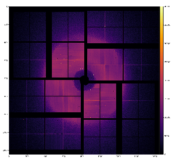
Quads' x0,y0 - center positions ONLY have been tuned as explained here:
1) Q0 and Q1 were moved together relative to the image center, because their geometry is constrained from optical metrology.
2) then Q2 and Q3 were moved independently in order to get consistent "to my eye" image relative to a set of drown circles.
Geometry for panels inside Q2 and Q3 is set from design geometry, and I do not feel that could do better job moving panels in quad.
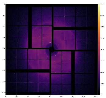
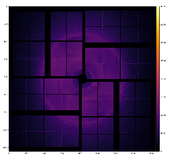
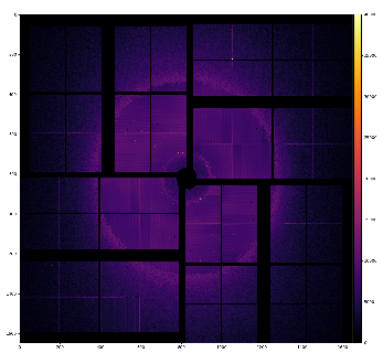
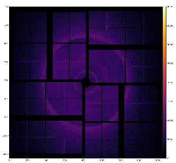
There are some regular alignment issues with this detector; if I tune nicely (with precision ~ pixel size) rings in the middle of radial range,
then internal and external rings may be misaligned. This may be due to small tilt of the detector or non-accounted z position of panels
w/o optical metrology.
Results
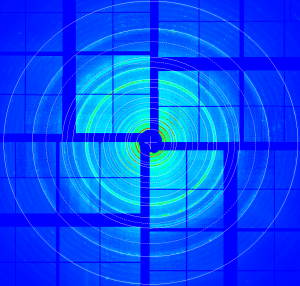
Resulting geometry for this data looks like on attached image.
All files are available under
- /reg/g/psdm/detector/alignment/epix10ka2m/calib-mfx-epix10ka2m-01-2018-11-15/2019-05-06-geometry-alignment/
Recommendation for further geometry improvement
The only reliable procedure to get correct detector geometry is an 3-d optical metrology of entire detector.
After that one would need to adjust precisely
1) detector center relative to image with rings
2) sample-to-detector distance
3) detector plane tilts.
References
- EPIX10KA2M References
- EPIX10KA
- EPIX10KA2M data images and geometry
- Production of calibration constants for multi-panel epix10ka detectors
- EPIX10KA2M Charge injection fit issue
- EPIX10KA2M issue with panel 6 in mfxc00318
- EPIX10KA2M issue with panel 12 in xcsc00118 2M.0
- Optical metrology of epix10ka2m.1 from 2020-02-25
- EPIX10KA panel flatness measurement
- Jungfrau and Epix10ka Calibration
- Detector alignment tool
- 2020-08-20-new-x-ray-detector-snaps-1000-atomic-level-pictures-second-natures-ultrafast
Overview
Content Tools