Setup for reading the ITkPixV1 quad module with YARR
Physical components:
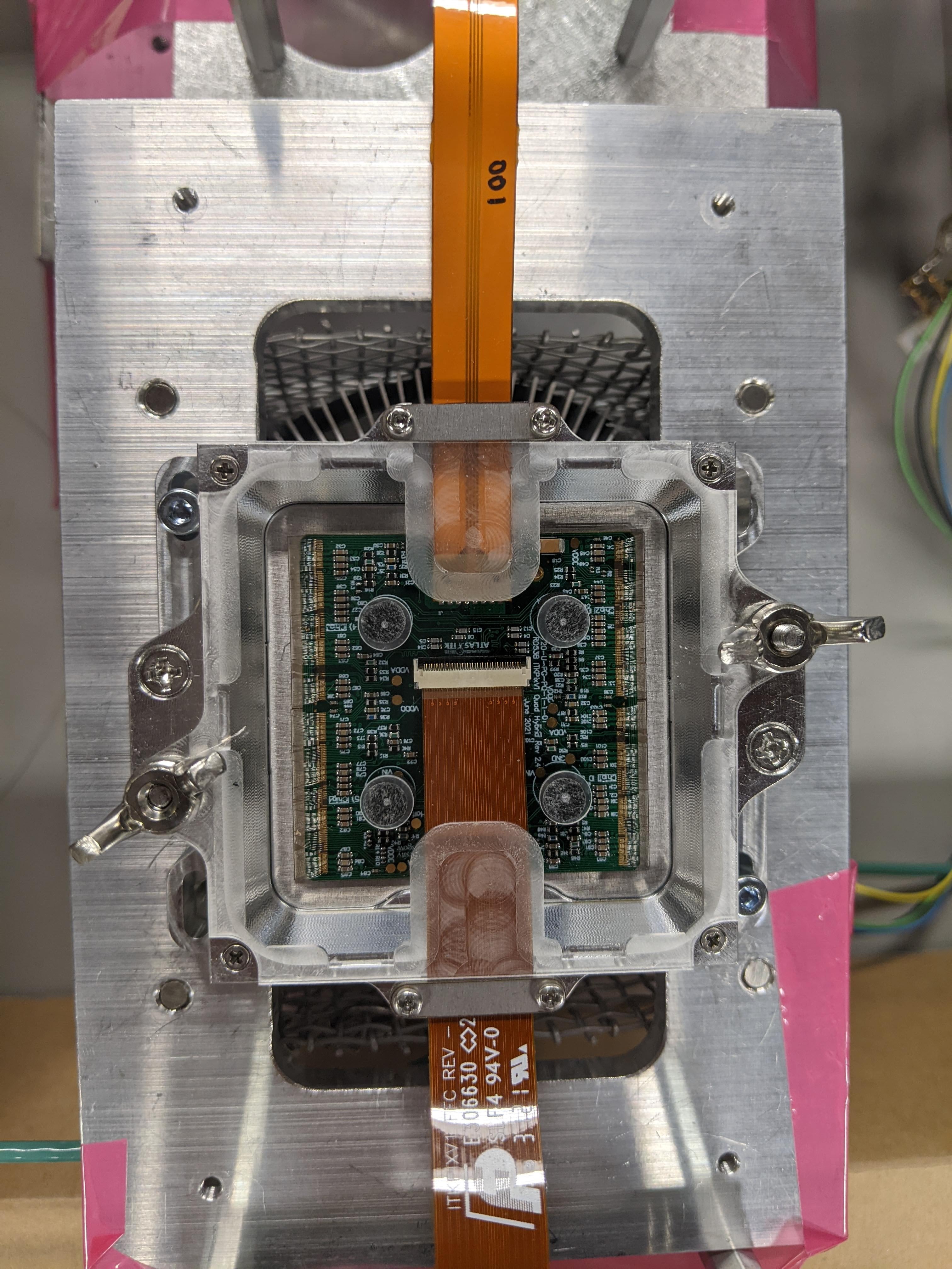
The module
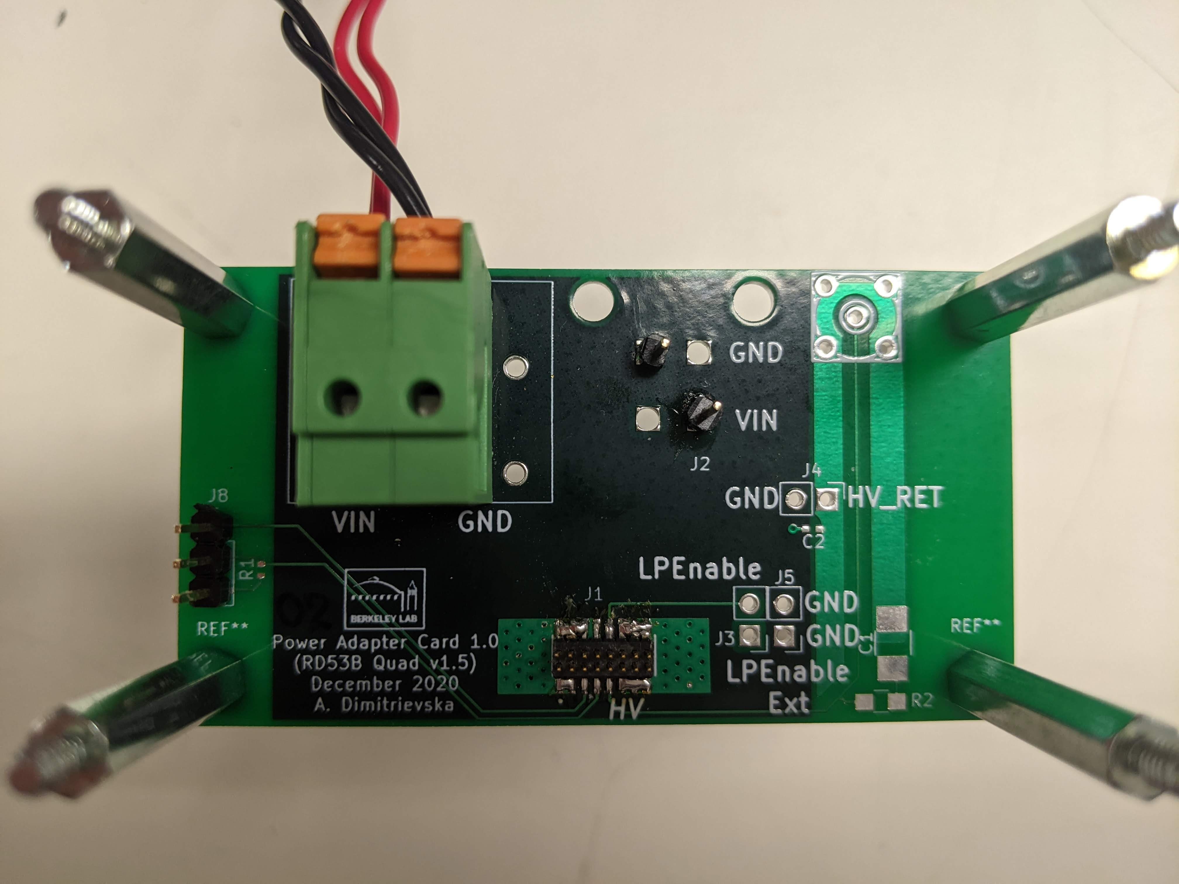
Power adapter
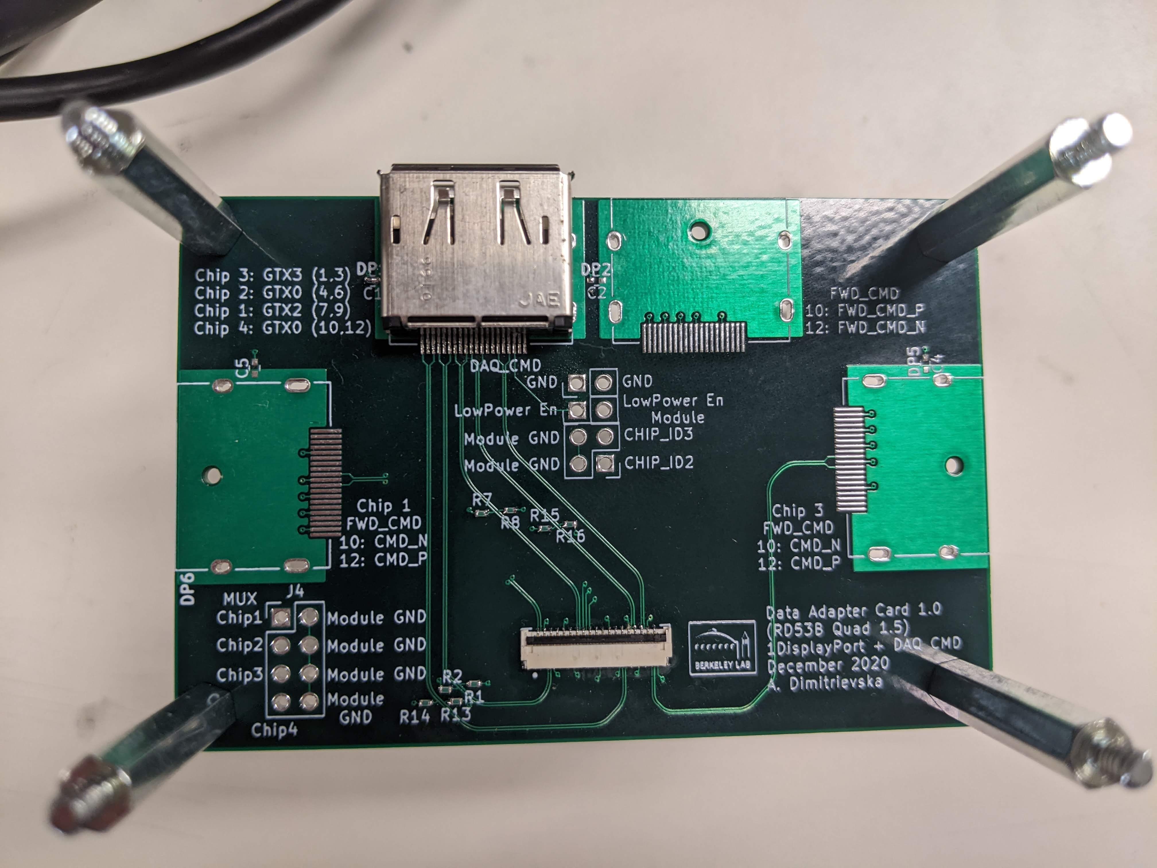
There are a few different types of data adapters. This is the one where all 4 chips are read through one DP adapter, so you'll need to use the 16x1 configuration in both software and firmware (you can check the firmware with ./bin/specComTest, and reflash the firmware if needed)
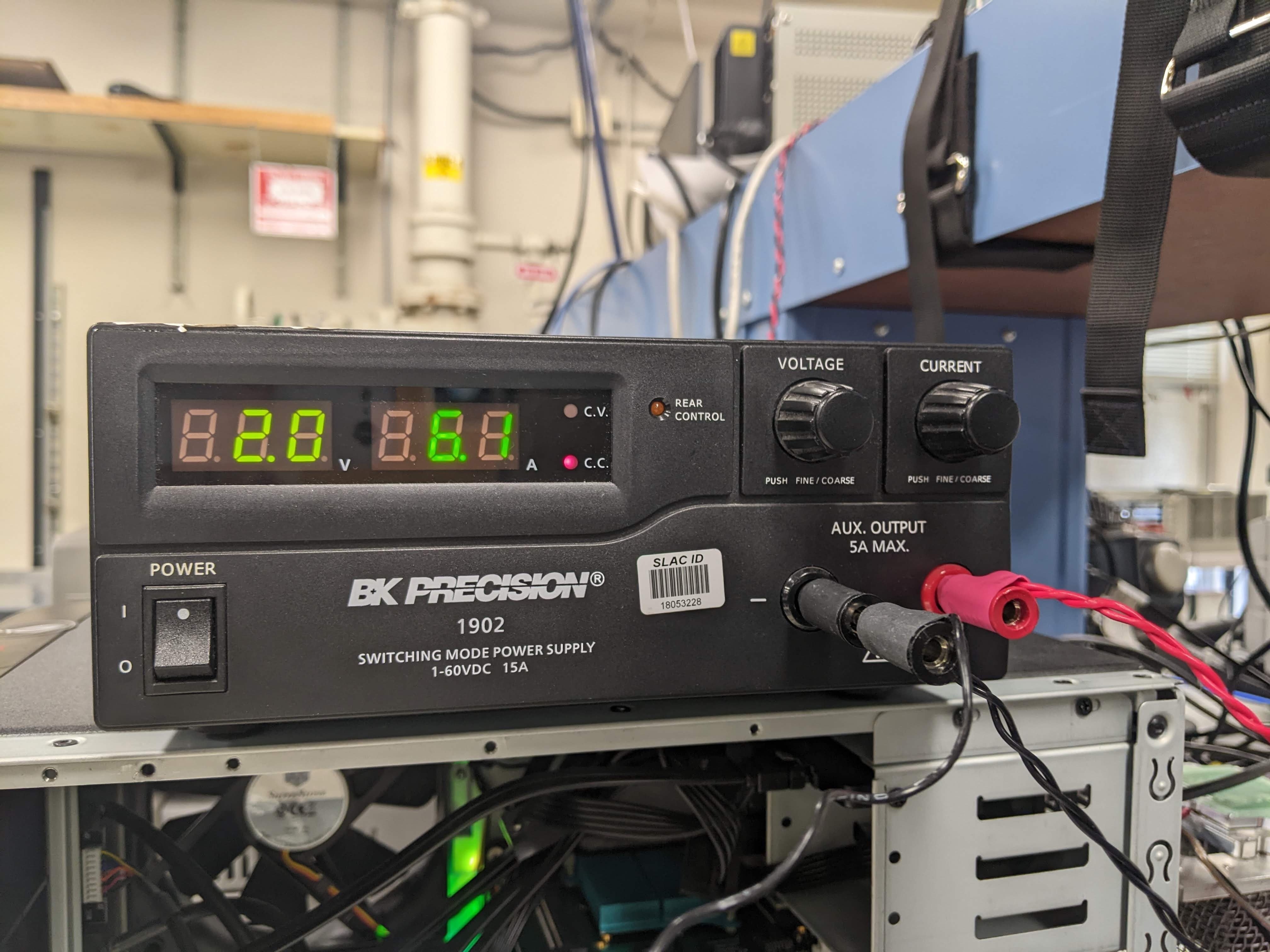
Power supply. Set to 2V (possibly more depending on loss in the wires) and 6.1A (1.526A per chip)
Running digital scans
Use the following tool to pull the config cards from the production database:
https://gitlab.cern.ch/berkeleylab/itk-pixel-module-software/itkpix-itkdb
python scripts/generateYARRConfig.py -sn 20UPGR91101015 -p L2
With fan + thermal pad, the module runs very hot at 36 - 38 C after configuration.
Digital scan:
bin/scanConsole -r configs/controller/specCfg-rd53b-16x1.json -c configs/20UPGR91101015/20UPGR91101015_L2_warm.json -s configs/scans/rd53b/std_digitalscan.json -p -n 1
Data transmission errors like the following:
[12:14:11:372][ error ][Rd53bDataProcessor][14352]: Expect new stream while NS = 0: 0100111001000110000100011100100100000010100111001001010001000011. Skipping block...
Can be solved by boosting the amplitude and preemphasis of the CMD driver. According to Timon, the default ones are sufficient for the SCC but not for the quad module because of the additional flex + adapter card. Timon's recommended quad settings are:
"CmlBias0": 800,
"CmlBias1": 200,
"SerEnTap": 1,
"SerInvTap": 1,
From tests, 3 chips on this module work pretty consistently with these settings while the last one (0x15448) always has some issues (only tested digital scans so far).
An explanation on the connectivity:
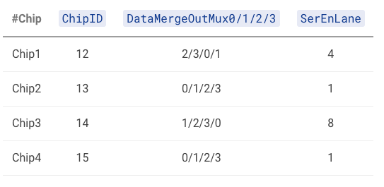
In each of the chip configs, you have a DataMergeOutMux variable which tells you the mapping between the internal data lanes and the external GTX lanes. For example, looking at the first row for chip1, this means that internal lane 2 is matched to GTX0, lane 3 to GTX1, lane 0 to GTX2, lane 1 to GTX3. Also, SerEnLane is set to the bit that will only enable the internal lane 0 (in this example, 4 = 0100). In particular, since we usually only use the internal lane 0 for scanning on a chip, this tells us that we should expect to see data on Chip1 GTX2, Chip2 GTX0, Chip3 GTX3, Chip4 GTX0.
Next, If you look at the top left of the data adapter, you can see the following information:
Chip#, External data lane, DP pins
Chip3: GTX3 (1, 3)
Chip2: GTX0 (4,6)
Chip1: GTX2 (7,9)
Chip4: GTX0 (10,12)
Note that these GTX and Chip maps are the same as what we expect from DataMergeOutMux. In the standard DP cable pin mapping, (1,3) is data0, (4,6) is data1, (7,9) is data2, and (10,12) is data3. That's why in our config file, we have: chip1 rx2, chip2 rx1, chip3 rx0, chip4 rx3. This means that as long as we are using this adapter with the same config files, we should expect 1 data lane per chip while scanning, with no data merging.
Setup for reading the ITkPixV1 quad module with YARR + type0 ring + pp0

Use the special ITkPix → type0 ring flex from Steven (not the one for RD53A)
This flex is designed so that as long as the ring is concerned, the data from chips 1, 2, 3, 4 are coming on lanes 0, 1, 2, 3, and not from lanes 2, 1, 0, 3 as we would have if we were using the ITkPix data adapter.
Of course there is still a mismatch between lanes on the ring side and the pp0, which luckily we have already mapped out here
Actually, you also need to swap the polarity for the CMD to get things to work - the exact reason for this is still unclear to me (Alex)
So for example, to run Q6: you need to make the following modifications:
In controller:
rxPolarity: 65535
txPolarity: 65535
In connectivity:
Chip1: rx0, Chip2: rx1, Chip3: rx3, Chip4: rx2
Then you can run with:
bin/scanConsole -r configs/controller/specCfg-rd53b-16x1_on_ring.json -c configs/20UPGR91101015/20UPGR91101015_L2_warm_on_ring.json -s configs/scans/rd53b/std_digitalscan.json -p -n 1
For Q6 (tested on Nov 7 2022), you can simultaneously run all 4 chips with a 1m DP cable at 640Mbps, though chip 1 will always have some failing pixels. Presumably this is a problem due to the ring (maybe one half of the data is disconnected on the flex?)
Tested positions so far
Position | Data channels on oscilloscope after turning on (no config) | Tested with YARR? |
Q4 | only data1- (data1+ broken?), data2+/- | |
Q3 | data1+/-, data2+/- | |
Q6 | data1+/-,data2+/- | All 4 chips working |
The fact that only 2 data channels show after just turning the module on seems to be normal for ITkPixV1. They correspond to the output lanes for chips 2 and 4 and might have to do with how these two chips are designated for data merging (more investigation needed).
Additional information:
The following page has some information on how the connectivity should be done: https://atlaswiki.lbl.gov/pixels/rd53bQuad/index
Also note that broadcast mode is chipID 16 for ITkPix instead of 8 for RD53A
Log for tests, with some maybe helpful debugging information, and some details on why we only see 2 data lanes on power-up: https://docs.google.com/document/d/1bvw4enmglHp-_2nJu62QusTybvB80sYdE18g9OzqC8U/edit?usp=sharing