...
We will irradiate sensots in August, in order to test the irradiated sensors during the October TestBeam.
Use of a PCB between sensor and chip:
here the idea is not put a PCB between the sensor and the chip, which would allow to shield the chip. It requires two bump bondings: sensor+PCB and PCB+chip. See Chris's presentation here: Radiation test with PCB
A drawing of the irradiation set-up can be found here: Proton_Irradiation 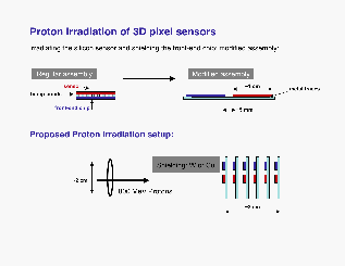
Simulation of the proposed LANL setup (by Heinz Vincke):
General layout:

PCB layout:

:
Shielding the sensor:
This was the initial idea, which was abandonned.
here is a drawing of principle for shielding the FE-I3 chips under proton irradiation:

Cold Bump Bonding:
here the sensor would be irradiated and then would be bump bonded to the FE-I3 chip, with cold bump bonds.
Use a staggered bonding:
see Philippe's presentation at the February 2008 3D Meeting: Proton_Feb2009
Design of a cool box for testing the sensors
Los Alamos irradiation facility
...
https://wnr-proposals.lanl.gov/index.shtml