![]()
Page History
| Tip |
|---|
The ePixUHR35kHz Megapixel Cameras project aims to provide modular detector blocks that can be configured into larger cameras in various structural configurations. The smallest building block is a 3x2 detector sensor module, which has a total of 3*2*192*168=193536≈200k pixels. Six of these (6*193536=1161216≈1M pixels) modules are assembled together into a 1 megapixel (1M) camera as shown below to the left. Four of the 1M cameras can then be assembled together, around a central beam pipe aperture, to form a 4M camera shown in the middle below. The largest configuration foreseen for this project is the 16M camera that consists of 16 of the 1M camera blocks as shown below on the right. |
1 megapixel (1M)
| |


6x 3x2 sensor modules:
- 6*3*2 = 36 ASICs
- 36*192*168 = 1,161,216 pixels
- 36*8 = 288 ASIC GT serial links
- 35 kfps: 288*1.975 = 568.8 Gbit/s
- 6 readout boards:
- 6 FPGAs & t ransceivers
- 6*12 = 72 fiber pairs
- 72*15 = 1080 Gbit/s
4 megapixel (4M)
|
|


4x 1M camera assemblies:
- 4*36 = 144 ASICs
- 144*192*168 = 4,644,864 pixels
- 144*8 = 1152 ASIC GT serial links
- 35 kfps: 1152*1.975 = 2275.2 Gbit/s
- 4*6 = 24 readout boards:
- 24 FPGAs & t ransceivers
- 24*12 = 288 fiber pairs
- 288*15 = 4320 Gbit/s
16 megapixel (16M)

16x 1M camera assemblies:
- 16*36 = 576 ASICs
- 576*192*168 = 18,579,456 pixels
- 576*8 = 4608 ASIC GT serial links
- 35 kfps: 4608*1.975 = 9100.8 Gbit/s
- 16*6 = 96 readout boards:
- 96 FPGAs & t ransceivers
- 96*12 = 1152 fiber pairs
- 1152*15 = 17280 Gbit/s
Table of contents
| Table of Contents | ||
|---|---|---|
|
Useful resources
- Jira Kanban board for this project
- TID-ID Edge Computing Systems
- Presentations:
- Concept Design summary presentation (Sharepoint)
- Restricted Content
HE project related information
Mechanical design
- Assembly
- ADD screen shots with key model views
Assembly procedure
Assembly procedure
| General | ASIC carrier module assembly | Readout module assembly | 1M assembly | 4M assembly |
|---|---|---|---|---|
|
|
|
Readout module assembly
|
|
|
4M assembly
- TODO
Toy model for inserting 1M module into the 4M crate
Multimedia name 4M-camera-assembly.mov
Sensor design
Due to asymmetry in the ASICs, the edges of the top row do not align exactly with the edges of the bottom row. The top row is shifted horizontally by 1.35 µm relative to the bottom row. The ASICs are spaced 19485 µm apart horizontally.


- Width (x): 60610 µm
- Height (y): 36525 µm
- x offset: 1166.695 µm
- y offset: 502.135 µm
- x distance: 178.74 µm
- x offset: 1168.045 µm
- y offset: 502.135 µm
- x offset: 178.74 µm
- y offset: 179.87 µm
- x offset: 1168.045 µm
- y offset: 502.135 µm
- x offset: 1165.695 µm
- y offset: 502.135 µm
Convert GDS to DXF:
- Download Klayout: https://www.klayout.de/
- Open the GDS
- Save it as DXF
Sensors for ASIC and systems characterization
There is a strong need to have sensors capable of detecting visible light during the characterization phase of the detector. This capability enables the use on lab, low power, LASER that can reproduce the fast timing and large charges that will be experienced during beam time use. X-ray sensor do have metallization in the entrance window to block visible light therefore existing sensor are not suitable
Solutions proposed
- Design mast on the 1x1 sensor in the production run
- It will take more than a year to have them and adds a step in the process, which adds risks to the production run
- Etch the metal away. Can be done in individual and prototype sensor (5x5mm)
- Only sensor for characterization would go through this step
- Can be done in existing sensor (have them available within a month)
- In the past we had issues removing the metal and CK's team will investigate this since it is believe this can be consistently done
- Decision is to make production runs with full metallization and process the sensors in house for characterization
|
|
Thermal Design
1MP Sensor Module Thermal Analysis by Component


| Epoxy Layer Thickness | Strongback Pillar Diameter | Thermal Pad Thermal Conductivity | Thermal Pad Thickness |
|---|---|---|---|
|
|
|
|


1MP Prototype
Determine the effectiveness of the thermal plate in drawing heat away from a heat source
Check cooling lines effectiveness
PowerPoint Overview: 1MPPrototypeThermocoupleMeasurements.pptx
CAD: 1MPTile
Set-Up & Enclosure
|
|
|
|


Components
- 4-piece foam box enclosure (see 4MP Cam Thermal testing.pptx for more info)
- 1MP Assembly Tool
- LabJack T7 with CB37 Terminal Board (see LabJackT7SetUp.ipynb to use LabJack over USB)
- Variable Power Supply
- Chiller w/coolant & tubing
- 14x Type K Thermocouples
3x2 Detector Sensor Module
| Visualization | Components | Circuitry | Thermal Analysis |
|---|---|---|---|
|
|
|
|

Readout Board
| Note |
|---|
| As of 8/7/24, this part of the prototype project is on hold, waiting for finalized cooling plate design |
| Visualization | Components | Circuitry |
|---|---|---|
|
|
|

Sensor design
The measurements below is based on the sensor design found in UHR_3x2_aug2024_overlay.GDS (restricted).
| Full sensor | Lower left corner | Between two ASICs at the bottom | Lower right corner | Between ASICs in the middle | Top left corner | Top right corner | |
|---|---|---|---|---|---|---|---|
| Image |
|
|
|
|
|
|
|
| Measurements |
|
|
|
|
|
|
|
Sensors for ASIC and systems characterization
There is a strong need to have sensors capable of detecting visible light during the characterization phase of the detector. This capability enables the use on lab, low power, LASER that can reproduce the fast timing and large charges that will be experienced during beam time use. X-ray sensor do have metallization in the entrance window to block visible light therefore existing sensor are not suitable
Solutions proposed
- Design mast on the 1x1 sensor in the production run
- It will take more than a year to have them and adds a step in the process, which adds risks to the production run
- Etch the metal away. Can be done in individual and prototype sensor (5x5mm)
- Only sensor for characterization would go through this step
- Can be done in existing sensor (have them available within a month)
- In the past we had issues removing the metal and CK's team will investigate this since it is believe this can be consistently done
- Decision is to make production runs with full metallization and process the sensors in house for characterization
Link to mechanical models: Dxf with the design
Electronics design for 3x2 sensor module
The electronics for the 3x2 sensor module is split into two parts; the ASIC carrier (left in the block diagram below) and the readout board (right in the block diagram). They are electrically connected together through a right-angle connector from the Samtec SEARAY connector family, which provides a total of 500 pins for signals and power. The ASIC carrier contains the 3x2 ASICs together with the 3x2 sensor and minimal amount of other components in order to reduce the size and therefore increase the sensitive area of the detector focal plane (the are which is covered by a sensitive sensor). All the active circuitry for interfacing and powering the ASICs is located on the readout board as well as the components for optical communication with the external back-end system.
More details about the electronics design for the 3x2 module can be found on a dedicated page: 3x2 Readout Overview
| Gliffy Diagram | ||||||||
|---|---|---|---|---|---|---|---|---|
|
| ePixUHR35kfps 3x2 Assembly | ePixUHR35kfps 3x2 Readout Board | ePixUHR35kfps 3x2 ASIC Carrier Board | |
|---|---|---|---|
| 3D view |
|
|
|
| Altium 365 project | ePixUHR35kfps-3x2-ASIC-carrier-board-C00 | ||
| Board tracking | PC_261_101_44_C00 | ||
| Dimensions (X x Y) | 59mm x 160mm | 60.69mm x 42mm | |
| STEP 3D model | ePixUHR35kfps-3x2-readout-board-PCB-2024-08-29.step | ePixUHR35kfps-3x2-ASIC-carrier-board-PCB-2024-08-16.step |
NOTE: If some of the images above are indicated as missing, please ensure that you are logged into Confluence and have access to the Board tracking pages where the images are stored.
Power
The system is designed to operate at 48 V nominally. There are separate supply connections for analog (APWR/AGND) and digital (DPWR/DGND) that are feeding different parts of the readout electronics, which can be used to have a low noise analog supply and a high-efficiency digital supply for example.
Power supplies
TODO, see
| Jira | ||||||
|---|---|---|---|---|---|---|
|
ePixUHR35kfps 1M Power Breakout Board
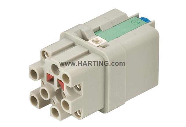
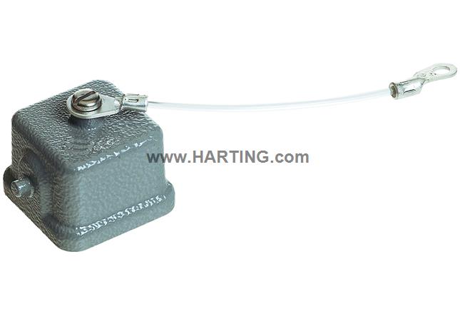
The 1M Power Breakout Board distributes the power to six 3x2 Readout Boards. It has two externally facing square Harting connectors, one for all the power and one for optional signals. Each power channel is individually fused with a socketed fuse to protect against catastrophic failures. Changing a fuse requires removal of the board from the 1M assembly, which has been done intentionally since blowing a fuse indicates something internal to the 1M assembly has gone wrong and requires expert investigation. The thermistor connections can be selected on the board through switches to which of the six 3x2 Readout Boards they connect to. Only one thermistor shall be connected per thermistor channel.
| Pin | Power connector (J1) | Signal connector (J2) - optional |
|---|---|---|
| 1 | Digital power (DPWR) | Timing input 0 (TIMING_IN_0) |
| 2 | Timing input 1 (TIMING_IN_1) | |
| 3 | Analog power (APWR) | Timing output 0 (TIMING_OUT_0) |
| 4 | Timing output 1 (TIMING_OUT_1) | |
| 5 | Digital ground (DGND) | Timing input 2 (TIMING_IN_2) |
| 6 | Digital ground (DGND) | |
| 7 | Analog ground (AGND) | Timing output 2 (TIMING_OUT_2) |
| 8 | Digital ground (DGND) | |
| 9 | Thermistor in (THERM_EXT_IN) | Spare connection (SPARE1) |
| 10 | Sensor ground (HV_GND) | Thermistor in (THERM_AUX_IN) |
| 11 | Thermistor out (THERM_EXT_OUT) | Spare connection (SPARE2) |
| 12 | Sensor biasing (SENSOR_HV) | Thermistor out (THERM_AUX_OUT) |
Board specific details
- See
Jira server SLAC National Accelerator Laboratory serverId 1b8dc293-975d-3f2d-b988-18fd9aec1546 key TIDIDECS-81 - The "Top" side of the board is facing the rear of the camera
- The "Bottom" side of the board is facing the inside of the camera and connects to the six 3x2 readout boards through the TFM connectors
| PCB | Assembly with connectors | |
|---|---|---|
Top |
| |
Bottom |
| |
Altium 365 project | ||
Board tracking | - | |
Dimensions (X x Y) | 110 mm x 110 mm | - |
3D files | TODO |
Connectors and parts
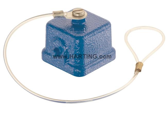
The two square Harting connectors on the Power Breakout Board above is separated into one for power and one for signal. They have different gender to avoid wrong connections. The power connector have a "protected" female connector on the cable side where voltages may be exposed on the pins. The tables below lists the components that are needed to assembly a full connector stack for the power and signal.
Power connector J1
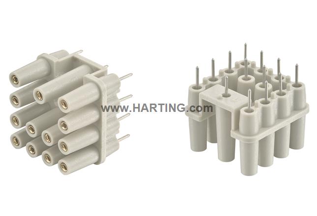
| Description | Harting part number | Quantity | DigiKey | Image |
|---|---|---|---|---|
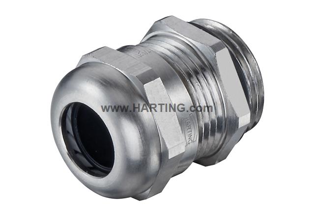
| PCB connector Han Q12/0 PCB Adapter | 09 12 012 9901 | 1 |
| |
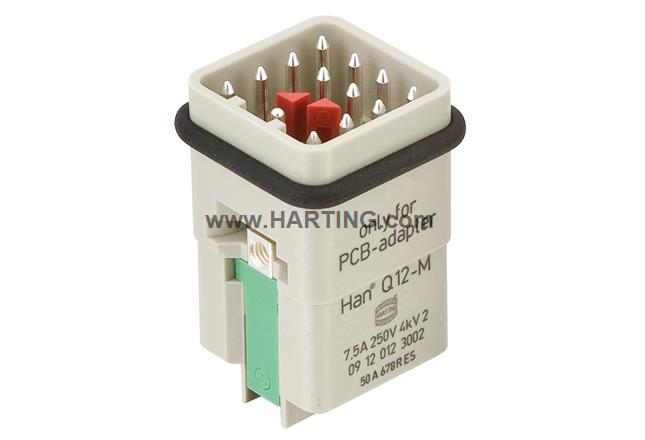
| Male PCB adapter Han Q12-M for PCB-Adapter | 09 12 012 3002 | 1 | 1195-1378-ND |
|
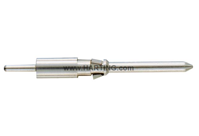
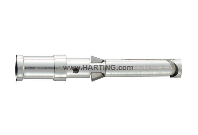
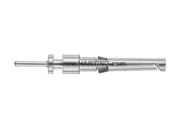
| Male pins for PCB adapter Han D-M-Kontakt f. Han Q12/0 LP-Adapter | 09 15 000 6191 | 12 | 1195-1575-ND |
|
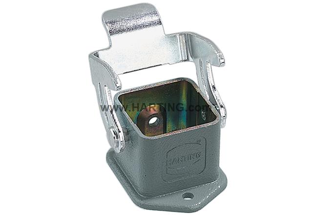
| Base flange Han 3A-HBM-SL | 09 20 003 0301 | 1 | 1195-1772-ND |
|
| Female crimp housing Han 12Q-SMC-FI-CRT-PE with QL | 09 12 012 3101 | 1 | 1195-1379-ND |
|
| Choose the crimp pins below to match the cable wire diameter (12 in total) | ||||
| Female crimp pins 1.0 mm² (18 AWG) | 09 15 000 6202 | x | 1195-1577-ND |
|
| Female crimp pins 0.75 mm² (18 AWG) | 09 15 000 6205 | x | 1195-1580-ND | |
| Female crimp pins 0.5 mm² (20 AWG) | 09 15 000 6203 | x | 1195-1578-ND | |
| Female crimp pins 0.14 mm² - 0.37 mm² (22-26 AWG) | 09 15 000 6204 | x | 1195-1579-ND | |
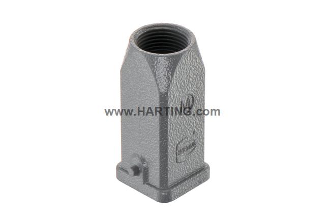
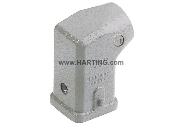
Only one hood needed | ||||
| Metal hood (grey) Han A Hood Top Entry 2 Pegs M20 | 19 20 003 1440 | 1 | 1195-3067-ND |
|
| Han A Hood Angled Entry 2 Pegs M20 | 19 20 003 1640 | x | 1195-3069-ND |
|
| Choose the cable gland below to match the external diameter of the cable | ||||
| Han CGM-M M20x1,5 D.5-9mm | 19 00 000 5080 | x | 1195-3032-ND |
|
| Han CGM-M M20x1,5 D.10-14mm | 19 00 000 5084 | x | 1195-3034-ND | |
| Han CGM-M M20x1,5 D.6-12mm | 19 00 000 5082 | x | 1195-3033-ND | |
| Han CGM-M M20x1,5 D.5-9mm/6-12mm | 19 00 000 5081 | x | 1195-3458-ND | |
Signal connector J2
| Description | Harting part number | Quantity | DigiKey | Image |
|---|---|---|---|---|
| PCB connector Han Q12/0 PCB Adapter | 09 12 012 9901 | 1 |
| |
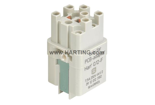
| Female PCB adapter Han Q12-F for PCB-Adapter | 09 12 012 3102 | 1 | 1195-1380-ND |
|
| Female pins for PCB adapter Han D F-ontact f. Han Q12/0 PCB adapter | 09 15 000 6297 | 12 | 09150006297-ND |
|
| Base flange Han 3A-HBM-SL | 09 20 003 0301 | 1 | 1195-1772-ND |
|
| Male crimp housing Han 12Q-SMC-MI-CRT-PE with QL | 09 12 012 3001 | 1 | 1195-1377-ND |
|
| Choose the crimp pins below to match the cable wire diameter (12 in total) | ||||
| Male crimp pins 1.0 mm² (18 AWG) | 09 15 000 6102 | x | 1195-1561-ND |
|
| Male crimp pins 0.75 mm² (18 AWG) | 09 15 000 6105 | x | 1195-1564-ND | |
| Male crimp pins 0.5 mm² (20 AWG) | 09 15 000 6103 | x | 1195-1562-ND | |
| Male crimp pins 0.14 mm² - 0.37 mm² (22-26 AWG) | 09 15 000 6104 | x | 1195-1563-ND | |
Only one hood needed | ||||
| Metal hood Han A Hood Top Entry 2 Pegs M20 | 19 20 003 1440 | 1 | 1195-3067-ND |
|
| Han A Hood Angled Entry 2 Pegs M20 | 19 20 003 1640 | x | 1195-3069-ND |
|
| Choose the cable gland below to match the external diameter of the cable | ||||
| Han CGM-M M20x1,5 D.5-9mm | 19 00 000 5080 | x | 1195-3032-ND |
|
| Han CGM-M M20x1,5 D.10-14mm | 19 00 000 5084 | x | 1195-3034-ND | |
| Han CGM-M M20x1,5 D.6-12mm | 19 00 000 5082 | x | 1195-3033-ND | |
| Han CGM-M M20x1,5 D.5-9mm/6-12mm | 19 00 000 5081 | x | 1195-3458-ND | |
Optional parts
Some optional parts that might be useful in some cases.
| Description | Harting part number | DigiKey | Image | Drawing |
|---|---|---|---|---|
| Cover with seal (gray) for female insert Han 3A Protect Cover, Sealing Die Cast f | 09 20 003 5425 | 1195-1792-ND |
| |
Cover without seal (gray) for male insert | 09 20 003 5426 | 1195-1793-ND | ||
| Cover with seal (blue) for female insert Han Ex-C for HCC Han 3A with seal | 09 36 003 5409 | 09360035405-ND |
| |
| Cover without seal (blue) for male insert Han Ex-C for HCC Han 3A | 09 36 003 5410 | 09360035410-ND |
Tools
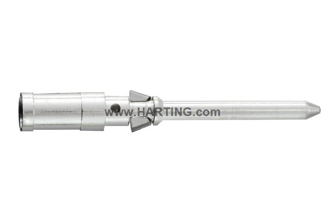
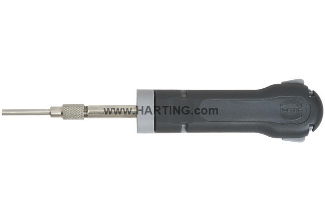
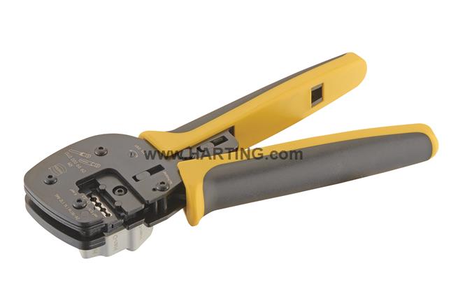
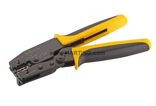
The pins that attach to the wires on the cable are crimped and required a specific tool for it listed below. A pin removal/extraction tool could also be useful in case a pin was inserted into the wrong slot.
| Description | Harting part number | DigiKey | Image | Drawing | Order | ||||||||||
|---|---|---|---|---|---|---|---|---|---|---|---|---|---|---|---|
| Small removal tool Removal Tool, Han D, Mini | 09 99 000 0052 |
| |||||||||||||
| Larger removal tool Removal Tool Han D | 09 99 000 0012 |
|
| ||||||||||||
| Universal crimp tool Han Hand Crimp Tool | 09 99 000 0110 |
|
| ||||||||||||
| Simple crimp tool Han CRIMP TOOL WITH LOCATOR | 09 99 000 0021 |
|
Power cable
There will be one power cable connecting to the Power connector J1 on the ePixUHR35kfps 1M Power Breakout Board that is routed to external power supplies at the installed location. The choice of cable is motivated and discussed in
| Jira | ||||||||
|---|---|---|---|---|---|---|---|---|
|
The cable is an igus CF9-05-12, which is a 12-conductor 0.5mm2 cable that is designed for heavy duty applications where the cable will be flexed in various direction, e.g. on a robotic arm. The outer jacket is made from TPE and the cable is specified to be halogen-free, PVC-free and Silicone-free. Some other important technical data about the cable:
- Datasheet
- Number of conductors: 12 x 20 AWG (0.5mm2)
- Stranded conductors of bare copper wires
Cores color code in accordance with DIN 47100
Outer jacket colored dark blue (similar to RAL 5011)
- A tear strip is moulded into the outer jacket (CFRIP)
- Outer diameter: 0.39 in (10 mm)
- Weight: 123 kg/km
- Min. bend radius, fixed: 1.18 in (30 mm)
- Min. bend radius, flexible: 1.57 in (40 mm)
- Nominal Voltage: 300/500V
- DigiKey: 4849-CF9-05-12-DS-ND
We assume a cable length of 50 ft (15.24 m) for now to give some headroom for the installation.
Resistance, voltage drop, power loss and weight
The voltage drop over the cable depends on the length and the current passing through the conductors. The 3x2 Readout Overview power map shows that the highest current is for the digital supply that requires 0.95 A when running at 48 V. For a 1M assembly this means a total current of 6*0.95 = 5.7 A and there are two conductors in the Power connector J1 for each supply that share the current. With this information, we can calculate the expected resistance of the conductors in the cable:
- Resistance equation: R = ρ * L / A
- ρ: resistivity of the material, copper at 20°C: ρ ≈ 1.7e -8 [Ωm]
- L: length of the conductor in [m]
- A: cross-sectional area of the conductor in [m2]
- R = 1.7e-8/0.5e-6*15.24 = 0.51816 Ω
- Voltage drop for two conductors -> half of 5.7 A current
- U = R*I
- U = 0.51816*5.7/2 ≈ 1.48 V
- Expected power loss in the cable: P = I2*R
- 5.7 A through two conductors at 48 V: 0.5 mm^2: P = (5.7/2)^2*0.51816 ≈ 4.2 W
- Total weight: 123*15e-3 = 1.845 kg
Sleeve for robotic arm
A flexible sleeve is used to guide the power cables and fiber optic cables for an application where the camera will be mounted on a robotic arm. A Triflex TRE sleeve from igus will be used and more details are available here. There are several sizes available and some of them are shown below as profiles with four gray power cables and four purple fiber optic cables (see below) placed inside for demonstration purposes. The cables are inserted into the sleeve through the slots at the top and bottom as shown below and there are tools available to ease with this.


Fiber
See
| Jira | ||||||
|---|---|---|---|---|---|---|
|
ASIC
The ePixUHR 100 kHz ASIC is used in this project. The main properties are:
- 192 (H) x 168 (V) pixels
- 100 um x 100 um pixel size
- 8 serial data outputs operating at up to ~6 Gbit/s
Resources:
- Confluence page (restricted)
- Glue used to bond the ASIC+SENSOR to the carrier board
- SP-120 silicone primer: https://nusil.avantorsciences.com/nusil/en/product/SP-120/silicone-primer
- CV-2943 thermally conductive, controlled volatility RTV silicone: https://nusil.avantorsciences.com/nusil/en/product/CV-2943/thermally-conductive-controlled-volatility-rtv-silicone
Size and measurements
These measurements are taken from a GDS file (ePixUHR_100kHz_4Julie.gds) that was opened in KLayout.
Link to mechanical models: Dxf with the design
Electronics design for 3x2 sensor module
The electronics for the 3x2 sensor module is split into two parts; the ASIC carrier (left in the block diagram below) and the readout board (right in the block diagram). They are electrically connected together through a right-angle connector from the Samtec SEARAY connector family, which provides a total of 500 pins for signals and power. The ASIC carrier contains the 3x2 ASICs together with the 3x2 sensor and minimal amount of other components in order to reduce the size and therefore increase the sensitive area of the detector focal plane (the are which is covered by a sensitive sensor). All the active circuitry for interfacing and powering the ASICs is located on the readout board as well as the components for optical communication with the external back-end system.
More details about the electronics design for the 3x2 module can be found on a dedicated page: 3x2 Readout Overview
| Gliffy Diagram | ||||||||
|---|---|---|---|---|---|---|---|---|
|


N/A
NOTE: If some of the images above are indicated as missing, please ensure that you are logged into Confluence and have access to the Board tracking pages where the images are stored.
Board-to-board connector
SAMTEC SEAF8/SEAM8 series connector will be used with 10x40=400 pins in one connector.
Photo of sample
(50 column version)


| title | Same connector but with 50 columns |
|---|
50 column
50 column with guide posts
Propagation delay
| Info |
|---|
Note: Due to the use of a right-angle connector there will be different path lengths for signals in different rows. See High Speed Characterization Report from Samtec. Table 16 on page 38 shows the propagation delay of the first row A (~100 ps) to the last row K (~180 ps) for different signal configurations. These propagation delay values have been assigned to the right-angle connector footprint pads for each row and will therefore be included in the propagation delay calculation in Altium when a trace is routed. The P and N signal of differential pairs should be placed in the same row to avoid skew between them. Timing critical signals should take into account the different propagation delays for the rows. |
| title | Click here to expand for propagation delay table... |
|---|
Propagation delays, cells with yellow color have been interpolated from the data in the report.
Row
Power
Power supplies
TODO, see
| Jira | ||||||
|---|---|---|---|---|---|---|
|
1M Power Breakout Board
- See
Jira server SLAC National Accelerator Laboratory serverId 1b8dc293-975d-3f2d-b988-18fd9aec1546 key TIDIDECS-81 - The "Top" side of the board is facing the rear of the camera
- The "Bottom" side of the board is facing the inside of the camera and connects to the six 3x2 readout boards through the TFM connectors
Top

Bottom

3D files
- STEP: HE-1M-power-breakout-assembly.step
- PARASOLID: HE-1M-power-breakout-assembly.x_t
ASIC
The ePixUHR 100 kHz ASIC is used in this project. The main properties are:
- 192 (H) x 168 (V) pixels
- 100 um x 100 um pixel size
- 8 serial data outputs operating at up to ~6 Gbit/s
Resources:
- Confluence page (restricted)
Size and measurements
These measurements are taken from a GDS file (ePixUHR_100kHz_4Julie.gds) that was opened in KLayout.


- Width (x): 19306.26 µm
- Height (y): 18674.7 µm
- Pad
- Width (x): 60 µm
- Height (y): 120 µm
- Pitch: 100 µm
- First pad location relative to lower-left corner
- x: 573.13 µm
- y: 45.095 µm
- Last pad location relative to lower-right corner
- x: 473.13 µm
- y: 45.095 µm
| title | Click here to expand for Altium footprint... |
|---|
| Full matrix | Lower left corner | Lower right corner | |
|---|---|---|---|
| Image |

|

|

| ||
| Measurements |
|
|
|---|
|
|
|
|
Block diagrams of camera configurations
The block diagrams have been created with Draw.io instead of the Gliffy integration in Confluence, which has major issue as soon as there are more than 100 items in the diagram it seems. It slows down the whole confluence page and it's near impossible to edit the diagram. There are also major limitations in the tools available in Gliffy, e.g. there doesn't seem to be a way to draw an arbitrary polygon or parallelograms.
Project Management
|
| Expand | ||||||||||||
|---|---|---|---|---|---|---|---|---|---|---|---|---|
| ||||||||||||
A footprint has been created in Altium Designer for the ASIC. The sizes and measurements listed above have been used and rounded to the nearest µm.
|


Block diagrams of camera configurations
The block diagrams have been created with Draw.io instead of the Gliffy integration in Confluence, which has major issue as soon as there are more than 100 items in the diagram it seems. It slows down the whole confluence page and it's near impossible to edit the diagram. There are also major limitations in the tools available in Gliffy, e.g. there doesn't seem to be a way to draw an arbitrary polygon or parallelograms.
Project Management
- Smartsheet
- PM Internal discussions
- LCLS-II-HE XES Detectors ePixHR10k PDR: https://indico.slac.stanford.edu/event/8884/
Reference documents from HE project
| Jira | ||||||
|---|---|---|---|---|---|---|
|
Reference documents from HE project
- Draft
- https://slac.sharepoint.com/:w:/r/sites/lcls/lcls-2-he/wd/PRD/LCLSII-HE-1.4-PR-0222.docx?d=w4eaaaca4a4774d7c9edee213070d7b51&csf=1&web=1&e=s1DVbb
- https://slac.sharepoint.com/:w:/r/sites/lcls/lcls-2-he/wd/ESD/LCLSII-HE-1.4-ES-1144.docx?d=w43d160d640204029b55ec6cdb5ed74b9&csf=1&web=1&e=Y2FrcG
- https://slac.sharepoint.com/:w:/r/sites/lcls/lcls-2-he/wd/FRS/LCLSII-HE-1.4-FRPR-11430222.docx?d=wd4f6f8b883b1463bae1eb198115994a0&csf=1&web=1&e=iX1UwD
- LCLSII-HE-1.4-ES-1144.docx
- LCLSII-HE-1.4-FR-1143.docx
- https://slac.sharepoint.com/:w:/r/sites/lcls/lcls-2-he/wd/ICD/LCLSII-HE-1.4-IC-0499.docx?d=w3073ea2890864e41a72ddd0b782baacc&csf=1&web=1&e=tUZam8
- LCLSII-HE-1.4-IR-0879.docx
- https://slac.sharepoint.com/:w:/r/sites/lcls/lcls-2-he/wd/ICD/LCLSII-HE-1.4-IR-08790880.docx?d=we5d9be1626e849549e24b797f6dd8b23&csf=1&web=1&e=blzNG6
- https://slac.sharepoint.com/:w:/r/sites/lcls/lcls-2-he/wd/ICD/LCLSII-HE-1.4-IR-08800881.docx?d=wb5875862dc0c4692aec36b61a37a4941&csf=1&web=1&e=nNlFBB
- Released
Jira tasks for the project
To do
| Jira | ||||||||||||
|---|---|---|---|---|---|---|---|---|---|---|---|---|
|
In progress
| Jira | ||||||||||||
|---|---|---|---|---|---|---|---|---|---|---|---|---|
|
Overview
Content Tools