...
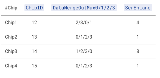
In each of the chip configs, you have a DataMergeOutMux variable which tells you the mapping between the internal data lanes and the external GTX lanes. For example, looking at the first row for chip1, this means that internal lane 2 is matched to GTX0, lane 3 to GTX1, lane 0 to GTX2, lane 1 to GTX3. Also, SerEnLane is set to the bit that will only enable the internal lane 0 (in this example, 4 = 0100). In In particular, since we usually only use the internal lane 0 for scanning on a chip, this tells us that we should expect to see data on Chip1 GTX2, Chip2 GTX0, Chip3 GTX3, Chip4 GTX0.
Next, If you look at the top left of the data adapter, you can see the following information:
Chip#, External data lane, DP pins
Chip3: GTX3 (1, 3)
Chip2: GTX0 (4,6)
Chip1: GTX2 (7,9)
Chip4: GTX0 (10,12)
The ITkPixV1.1 Digital Quad hybrid V1.5 schematics indicates that only two GTX output of each chip are physically connected to the module ZIF. The quad module ZIF interface and further connectivity details of the to Quad Readout Adaptor with 1 DP connector serving 1 line per FE (schematics) via straight-through module Q/C flex is captured in the "ITkPixV1-Quad" tab of the RD53A Ring Connectivity Stanford Drive GoogleSheet. The Quad Readout Adaptor further down selects the data GTX channels to only keep one data GTX per FE to form the 4 channels on the single DP connector:
| Module | Readout adaptor | Alex* | ||
|---|---|---|---|---|
| Chip | GTX | DP lane | DP pin | DP Pin |
1 | 2 | 1 | 4,6 | 7,9 |
| 2 | 0 | 0 | 1,3 | 4,6 |
| 3 | 3 | 2 | 7,9 | 1,3 |
| 4 | 0 | 3 | 10,12 | 10,12 |
- There is a discrepancy between the schematics trace by SD and Alex' original empirical recording. To be resolved. When DAQ connects to adaptor, the DP-DP cable flips lane 0↔3.
Note: Note that these GTX and Chip maps are the same as what we expect from DataMergeOutMux. In the standard DP cable pin mapping, (1,3) is data0, (4,6) is data1, (7,9) is data2, and (10,12) is data3. That's why in our config file, we have: chip1 rx2, chip2 rx1, chip3 rx0, chip4 rx3. This means that as long as we are using this adapter with the same config files, we should expect 1 data lane per chip while scanning, with no data merging.
Some notes from schematics reading: For the readout adaptor in module QC setup with ZIF facing the module ZIF, the ZIF pin orders are reversed between two sides when connecting with a straight QC flex. This looks like is handled coherently (unlike RD53A) between the module and adaptor. Single polarity also preserved p->p,n→n for all data lines, but it looks like CMD deliberately flipped polarity at the adaptor as needed for ITkPix vs RD53A.
Setup for reading the ITkPixV1 quad module with YARR + type0 ring + pp0
...