Introduction
The following discussions apply to the CSpad family of detectors, but all of the specific discussions and tests were done with the CSpad140k detector. If, while reading this page, you would like to refer to the CSpad 2.3M or CSpad 140k configurations, an image of each configuration GUI screen is given at the bottom of this page in child pages.
Placing the integration window
Before going into detail, it is necessary to describe the pixel architecture of the cspad. For this purpose, I have borrowed a figure from a paper presented at the SPIE conference by Philip Hart, et. al.
![]()
Holes generated by the incidence of the x-ray photons are collected at every pixel's charge sensitive amplifier. The resulting output voltage of this amplifier is then sampled and held for digitization. The time during which the detector is sensitive to x-rays also known as integration window is established by the release of the reset switch on the charge sensitive amplifier and then ended by the opening of the switch for the sample and hold capacitor. After some time to allow the sample and hold output to settle, the external ramp signal starts falling and the counter starts clocking. When the external ramp level and the pixel signal level match, the comparator fires and the counter stops, resulting in the digital value for output (single slope ADC principle).
All parameters that affect the timing of the CSPAD detectors are clocked by the 125 MHz clock with a cycle time of 8 nanoseconds except the "Run Delay" in the CSpad 2.3M which is clocked at 119 MHz with a cycle time of 8.40336 nanoseconds.
The duration of the integration window is determined by the "Int Time" parameter in the configuration. A typical setting of 5000 commands an integration window of 40 microseconds. To really understand the integration window we should look at the weighting function studies done by Sven Herrmann, Gabriella Carini, et. al. in various hutches at LCLS.
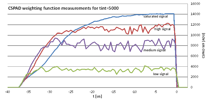
The weighting function shows the response at various flux levels vs time. These curves are for a 40 microsecond integration window. The 40 microsecond digital integration window starts with the command to release the amplifier reset, at -40 microseconds in the above curves. Since we now use the analog reset, several microseconds elapse from the time we command the release of the reset and when some response is seen in the curves. In the discussion below we are talking about the digital window, but remember that the actual performance of the detector is determined by the curves shown above.
Note also, that since the all the FPGA times start with a count of zero, we should add one to the settings before using them in calculations.
The position in time of the integration window relative to the event code 140 timing, is the sum of three things.
In the CSpad 140k, the position of the run trigger itself makes the first contribution. We normally set it at 500 microseconds after the 140 event code.
The second is the "Run Trig Delay" on the 140k and the "Run Delay" on the CSpad 2.3M. For the 140k it is typically has been 11020, or 88.168 microseconds. In the CSpad 2.3M, the "Run Delay" should include the 500 microseconds of the 140k run trigger, because there is no run trigger for the 2.3M.
These first two contributions are not part of the actual acquisition cycle, but determine the start of it.
The next contribution is the "Acq Delay", clocked by the 125 MHz clock counted down by 128, so in units of 8ns * 128, or 1.024 microsecond. A typical setting of 280, yields 287.744 microseconds.
Applying the numbers on this places the start of the analog integration window at:
500 + ((11020+1)*0.008) + ((280+1)*1.024) = 875.912 microseconds, with a 40 microsecond window ending at 915.912 microseconds.
This would place the FEL (~896 microseconds) 20 microseconds into the window and 20 microseconds from the end.
When the stale stand-alone evr issue raised it's head, CXI scientists scanned and then used these numbers.
400 + ((22580+1)*0.008) + ((280+1)*1.024) = 868.3912 microseconds, with a 40 microsecond window ending at 908.3912
This would place the FEL 27 microseconds into the window and 13 from the end. While this looks better in the curves above than our previous settings, it might be better still to go to about 30 microseconds into the window and 10 from the end.
While I am not suggesting changing the run trigger timing, changing the "Run Delay" to reflect this moving of the FEL enough later in the window to put the FEL at about 30 microseconds into the window should be given serious consideration. Specifically, that would mean setting the "Run Trig Delay" to 9781, or 78.256 microseconds.
This would bring the timing to:
500 + ((9781+1)*0.008) + ((280+1)*1.024) = 866 microseconds
Calculating the acquisition cycle time
The first contribution to the cycle time is the "Acq Delay" mentioned above as (280+1) * 1.024 microseconds, before the integration window.
The next contribution is the integration window itself, currently set at 40 microseconds, determined by the "Int Time" configuration parameter.
After the integration window ends with the opening of the sample and hold switch, the logic waits "Dig Delay" in units of 8ns. This is for the sample and hold to stabilize before we start the A to D. A setting of 960 yields 7.69 microseconds.
Next the ramp into the comparator is started. It steps "Dig Count" +1 times with a step interval of "Dig Period" +1 in units of 8ns. The ramp completes its whole course so that all pixels, even those who are saturated with photons will see their comparators fire. This total ramp time is thus ("Dig Count" + 1) * ("Dig Period"+1) in units of 8ns. A maximum value "Dig Count" of 0x3fff and a "Dig Period of 25 yields a count time of 3,407.9 microseconds.
Using these number we get:
((280+1)*1.024) + 40 + ((960+1)*0.008) + ((0x3fff+1)*(25+1)*0.008) = 3743.304 microseconds.
Conveniently for our purposes, the firmware in the front end includes a method to count the acquisition cycle time when using these numbers.
acqTimer(858546)(6868368ns), so 6868.368 microseconds
Using a shorter "Dig Period" setting:
((280+1)*1.024) + 40 + ((960+1)*0.008) + ((0x3fff+1)*(12+1)*0.008) = 2039.368 microseconds.
Yields:
acqTimer(645567)(5164536ns), or 5164.536 microseconds
In both cases, the cycle time includes 3.125 milliseconds of unaccounted time, so far, some of which goes to reading out the data.
The data readout time is related to "Read Clk Set", "Read Clk Hold" and "Row/Col Shift." Every block has to be read out serially: a total of 26x185 pixels for every pixel we have to clock 14 bits of data and do at least one row/col shift. So every pixel needs at least 14*(read_clock_set + read_clock_hold +2) + 2*(row/col_shift+1) + 4 clock cycles.
For the CSpad140k, "Read Clk Set" and "Read Clk Hold" values of 1 and "Row/Col Shift" value of 3:
(14*(1+1+2) + 2*(3+1) + 4) * 26 * 185 * 0.008 = 2616.64 microseconds, which still leaves 508.36 microseconds of undefined overhead in the cycle time.
For the CSpad 2.3M, because the data is read out over copper LVDS links, we need to use a "Read Clk Set" value of 2.
Timing for the DAQ trigger
Both detectors need a DAQ trigger to label events that the DAQ system wants to save. All the timing of the integration window position depend only on the run trigger or the arrival of the specified event code. The DAQ trigger only specified that the DAQ system wants this frame, so ti's arrival time is not critical. The DAQ trigger must arrive after the run trigger, but no more than 500 microseconds after it. The software looks at the configured delay of the run trigger, and adds 250 microseconds to that for the setting of the DAQ trigger delay. This scheme means that you set the run trigger delay to set the position of the integration window and the set the DAQ trigger delay to the same value, so the software will place the daq trigger in the middle of the window.
Overview
Content Tools