Setup for reading the ITkPixV1 quad module with YARR
Physical components:

The module


Power adapter


There are a few different types of data adapters. This is the one where all 4 chips are read through one DP adapter, so you'll need to use the 16x1 configuration in both software and firmware (you can check the firmware with ./bin/specComTest, and reflash the firmware if needed)

Power supply. Set to 2V (possibly more depending on loss in the wires) and 6.1A (1.526A per chip)
...
From tests, 3 chips on this module work pretty consistently with these settings while the last one (0x15448) always has some issues (only tested digital scans so far).
An explanation on the connectivity:
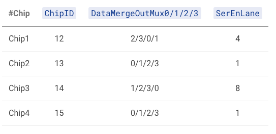
In each of the chip configs, you have a DataMergeOutMux variable which tells you the mapping between the internal data lanes and the external GTX lanes. For example, looking at the first row for chip1, this means that internal lane 2 is matched to GTX0, lane 3 to GTX1, lane 0 to GTX2, lane 1 to GTX3. Also, SerEnLane is set to the bit that will only enable the internal lane 0 (in this example, 4 = 0100). In particular, since we usually only use the internal lane 0 for scanning on a chip, this tells us that we should expect to see data on Chip1 GTX2, Chip2 GTX0, Chip3 GTX3, Chip4 GTX0.
Next, If you look at the top left of the data adapter, you can see the following information:
Chip#, External data lane, DP pins
Chip3: GTX3 (1, 3)
Chip2: GTX0 (4,6)
Chip1: GTX2 (7,9)
Chip4: GTX0 (10,12)
Note that these GTX and Chip maps are the same as what we expect from DataMergeOutMux. In the standard DP cable pin mapping, (1,3) is data0, (4,6) is data1, (7,9) is data2, and (10,12) is data3. That's why in our config file, we have: chip1 rx2, chip2 rx1, chip3 rx0, chip4 rx3. This means that as long as we are using this adapter with the same config files, we should expect 1 data lane per chip while scanning, with no data merging.
Additional information:
The following page has some information on how the connectivity should be done: https://atlaswiki.lbl.gov/pixels/rd53bQuad/index
Also note that broadcast mode is chipID 16 for ITkPix instead of 8 for RD53A
Ongoing log for tests: https://docs.google.com/document/d/1bvw4enmglHp-_2nJu62QusTybvB80sYdE18g9OzqC8U/edit?usp=sharing