Search/Navigation:
Related:
SLAC![]() /EPP
/EPP![]() /HPS Public
/HPS Public![]()
Jefferson Lab![]() /Hall B
/Hall B![]() /HPS Run Wiki
/HPS Run Wiki![]()
S30XL-LESA/LDMX
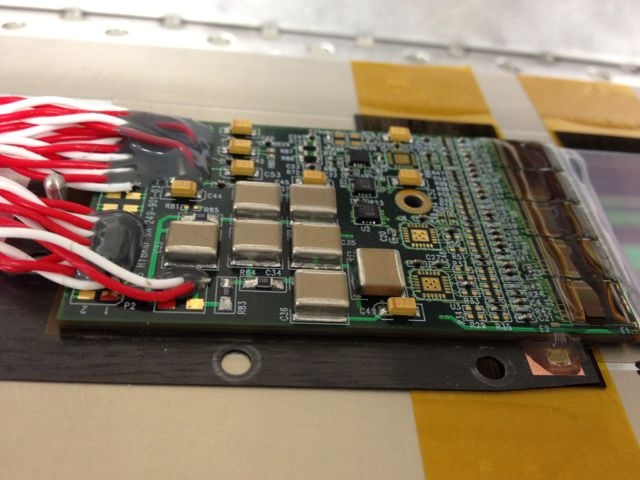
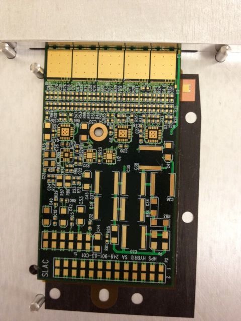
Test Run 2012 | HPS 2014/L4-6 hybrid | Layer 0 Hybrid | |
|---|---|---|---|
Hybrid schematics | draft , final | board-page | |
Hybrid Layout | draft , final | Drawings of hybrid (pdf), Model of hybrid (Layer0 Hybrid.dwg) Complete model of Layer 0 components (Layer0 Module 2018.dwg) Pigtail wire gauges (includes all SVT cables) heavyp_cables_updated.xlsx | |
PADS |
7 Comments
Tim Nelson
It seems that the biasing filtering for the detector still needs to be defined. In particular, the multistage filter uses 100V caps (we need at least 500V), 100uF capacitances (unrealistically large) and no resistances. In the past we have used 1K resistors and the largest surface mount capacitances we can get in the voltages we need. Looking at what AVX and Johanson have, it looks like 220 or 470 nF at 500V or more are the best we can do (and probably just fine).
Tim Nelson
An issue here is the drivers for transmitting data between the hybrid and the RTM: we need to make sure they are capable of driving those lines. In order to do that, we need to specify the length of cable that will be needed to connect the two. This depends upon the location of the DAQ and the cable routing that will be used. How long can those lines be as designed?
Omar Moreno
Comments and Questions from SCIPP:
Tim Nelson
Just waking up with coffee and don't have prints in front of me, but I can clarify a few of these:
4.) Perhaps it didn't come through on the phone, but in the meeting I explained that this was a typo: the support shall be connected to the input reference for the input transistor. I have changed the spec and apologize for the confusion. Too much KPiX on the brain!
5.) I believe we can go directly from the back side of the hybrid to the sensor, but this depends on layout details. What I really meant is that:
6.) Good point. BTW, we may not be able to get the supplies above 350V, but we'll see soon enough.
7.) See (4). Also... please try to make comments on the mechanical and cooling spec page also where relevant, as I don't want Ryan and Marco to have to watch both pages.
8.) The is a religious war. I've NEVER seen a project where encapsulating turned out to be a bad thing in the end. conversely, I've seen many projects where not encapsulating turned out to be a fatal flaw. So... I'll confess that I am an encapsulator. Many batches of Sylgard 186 were tested for ionic impurities and it was used for CLEO-II, CDF Layer 00 and ISL, and CMS. It's the best stuff there is. It may outgass too much, and then we'll just have to learn to be careful. It's not about shaking, it's about incidental contact.
9.) Preaching to the choir.
10.) Some reference for the problems you refer to would be helpful. We've flattened sensors this long before, but they were somewhat narrower. We should measure some on the OGP and see how bowed they are.
Omar Moreno
More Comments from SCIPP:
11. Sensor supports and nearby conductors:
Conductive sensor frame and support members should not have unnecessarily close proximity to the strips to limit capacitance to EMI carrying objects. The close conductive frame members for a sensor or sensor stack should have common bonding ties to each other, and be isolated as a group from the main cabinet and frame. A single bond tie, low AC impedance @ 20 MHz, should bond at the Analog 1.25 V supply at the rear edge or at the power entry to the PCB.
12. Analog power necking:
The ADA4938 diff amp allows an analog power plane neck strategy. The 1.25 V referencing plane for the group of APVs servicing one sensor can have a single point tie to the rest of the PCB circuit nodes. The ADA4938 should rest in this front power plane, since its drivers exactly balance their differential drive current, and should disturb the power plane minimally.
13. Front power plane with power islands:
For the demanding mixed signal challenge of sensor strips, a single power plane with power island strategy works well. The power plane should be the Analog 1.25 V supply, since the front transistors reference here, and this will avoid referencing through capacitors. The internal PCB plane should be 2 ounce copper uncut across the group of APVs to a sensor. The two other power sources, 0 V and 2.5 V, should be drawn as "islands", that is, a power plane in the area of a chip to tie the bypass cap and the IC pad together, but the local island serviced by an inductive trace. The trace should be sized to carry the servicing currents, but need be no larger. In series with the power trace, provision should be made for a jumper or air-core inductor. The goal is to force AC currents between chips into a single plane, so that the currents balance locally, and have less EMI.
The "ground pour" layout tool needs to be used carefully. Ground pour could used in the area of a power island, but the island needs to stay contained from jumping the island border. the intention is that currents between islands flow only in the A_1.25 plane.
The 3 analog power connections to the APV sensor group should be single point and grouped together in the PCB layout. The ADA4938 power should also be single point in the same area. A series jumper would be useful here on each supply.
14. Sensor backplane referencing path:
The sensor backplane tie to the PCB A_1.25 plane should be near the front APV area. The tie needs to be low impedance @ 20 MHz. This excludes simple wires or narrow traces as the bond technique.
Tim Nelson
Thanks for the layout comments. (11) is something I'm particularly concerned about also, and we'll have to work together to optimize. As it stands, we have conductive members only underneath the silicon. I NEVER place anything conductive against the strips after experience with CLEO-II in the early 90's where we changed to Kevlar composite to solve a problem that was too late to solve with a design change.
Tim Nelson
Ryan... can we add temperature measurement on the hybrids? I'm a bit concerned that we need to keep track of chip temperatures as part of our conditions data.