SLAC/EPP/HPS Public Jefferson Lab/Hall B/HPS Run Wiki S30XL-LESA/LDMX
Signal flange board
Board schematics
board page
Board layout
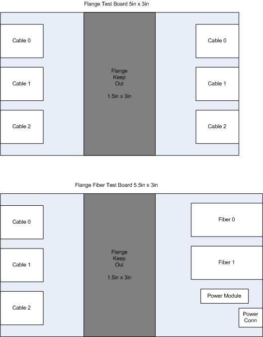
conceptual layout